![]()
Download this complimentary Whitepaper today!
This whitepaper provides engineers and researchers with a technical framework for understanding how thermal behavior is changing in advanced semiconductor systems. As devices scale into three-dimensional architectures with thinner layers, higher power densities, and increasingly complex material stacks, heat transport becomes confined, interface-dominated, and highly sensitive to small variations in structure and processing. These shifts are making accurate thermal characterization increasingly important for design workflows, model validation, and long-term reliability in modern electronic systems.
What you will learn about:
-
Why classical bulk thermal assumptions break down at nanometer-scale film thicknesses and how this affects thermal conductivity and device-level modeling accuracy.
-
How emerging architectures such as 3D integration, gate-all-around transistors, and backside power delivery networks reshape vertical heat flow and create buried thermal bottlenecks.
-
Why thermal boundary resistance at bonded interfaces, TIM layers, and dielectric stacks has become a first-order driver of performance limits and reliability risks in advanced packages.
-
How a thermal-first design workflow based on measured, scale-appropriate material properties improves model accuracy, reduces uncertainty, and helps prevent costly late-stage redesigns.
Click “LOOK INSIDE” to Download Now.
LOOK INSIDE
IEEE Spectrum and Wiley are proud to bring you this white paper, sponsored by Laser Thermal.
More Information
As semiconductor architectures evolve beyond classical transistor scaling into heterogeneous integration, chiplet-based design, and true 3D stacking, heat management has shifted from a secondary design consideration to a defining constraint on system performance.
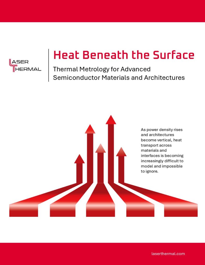
At the same time, power densities continue to rise while materials and device layers become thinner, creating thermal pathways that are increasingly confined and interface-dominated. In these regimes, heat transport depends strongly on thin films, bonded interfaces, and buried layers that control vertical heat flow inside modern electronic systems.
This guide examines how semiconductor scaling, advanced packaging, and emerging materials are reshaping thermal behavior across modern devices. It explores how these architectural changes amplify the importance of thermal conductivity, thermal boundary resistance, and spatial variability, and why accurate thermal measurement is becoming essential for validating models, guiding design decisions, and ensuring reliable system operation.
Sponsored by
Partnered with
IEEE Spectrum Magazine, the flagship publication of the IEEE, explores the development, applications and implications of new technologies. It anticipates trends in engineering, science, and technology, and provides a forum for understanding, discussion and leadership in these areas.