Download this complimentary Infographic today!
This Infographic provides scientists and engineers with essential information on advanced microscopy solutions for nanophotonics research, enabling you to accelerate nanofabrication workflows and understand critical structure-property relationships in photonic materials.
What you will learn about:
- How multi-scale electron microscopy accelerates nanophotonic device development from design to manufacturing
- Integration of FIB-SEM systems for rapid prototyping with in situ verification, reducing development cycles from months to weeks
- Real-world applications including plasmonic nano-antennas, smartphone optics, and optical switches
- Correlative imaging workflows that connect device-level performance to nanometer-scale structural features
Click ‘LOOK INSIDE’ to Download Now.

More Information
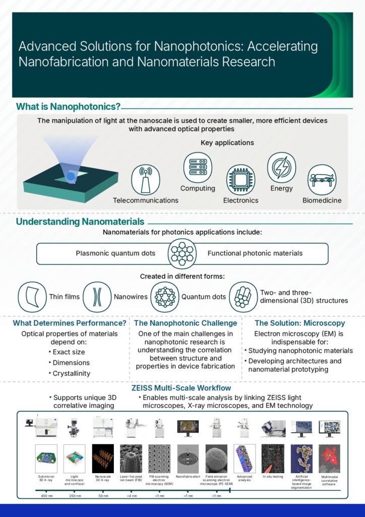
Nanophotonics—the manipulation of light at the nanoscale—is transforming telecommunications, computing, electronics, energy, and biomedicine. Creating high-performance nanophotonic devices requires understanding how exact size, dimensions, and crystallinity affect optical properties. One of the main challenges in nanophotonic research is understanding the correlation between structure and properties during device fabrication. ZEISS multi-scale electron microscopy workflows provide integrated solutions spanning from light microscopy through X-ray microscopy to electron microscopy, enabling researchers to study nanophotonic materials, develop architectures, and accelerate prototyping. This infographic demonstrates how correlative imaging approaches bridge the gap between atomic-scale surface structure and millimeter-scale device performance, with case studies showing dramatic reductions in development time, prototype iterations, and manufacturing costs.
Brought to you by
Sponsored by